Power Delivery
Reimagined for AI
PowerLattice is reimagining power delivery for next-generation AI accelerators with the industry's first power delivery chiplet

AI accelerators and GPUs, pushing past 2,000 watts per chip, are creating a power crisis for data centers, hitting a "power wall." Current power delivery methods are inefficient, wasting energy and hindering performance
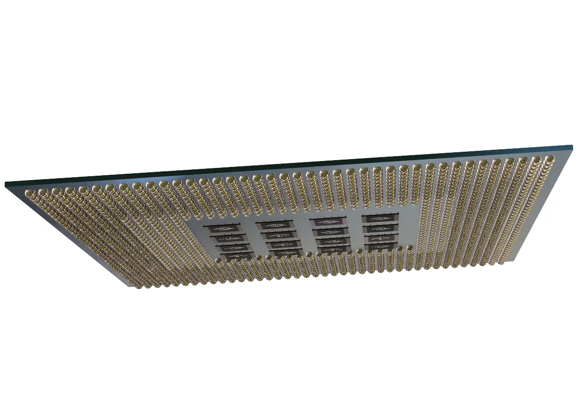
PowerLattice’s solution breaks through the power wall by moving voltage regulation directly into the processor package, just a few hundred micrometers, rather than inches, from the accelerator or GPU die. This tight coupling saves power and significantly reduces conduction loss on PCB and package substrate, leading to less heat dissipation, higher power ceiling for compute, and more AI computing per rack.
PowerLattice provides a true monolithic solution with a vertical design that unifies our miniaturized proprietary on-die magnetic inductors, advanced control circuit innovations, and a programmable software layer in one compact silicon die.
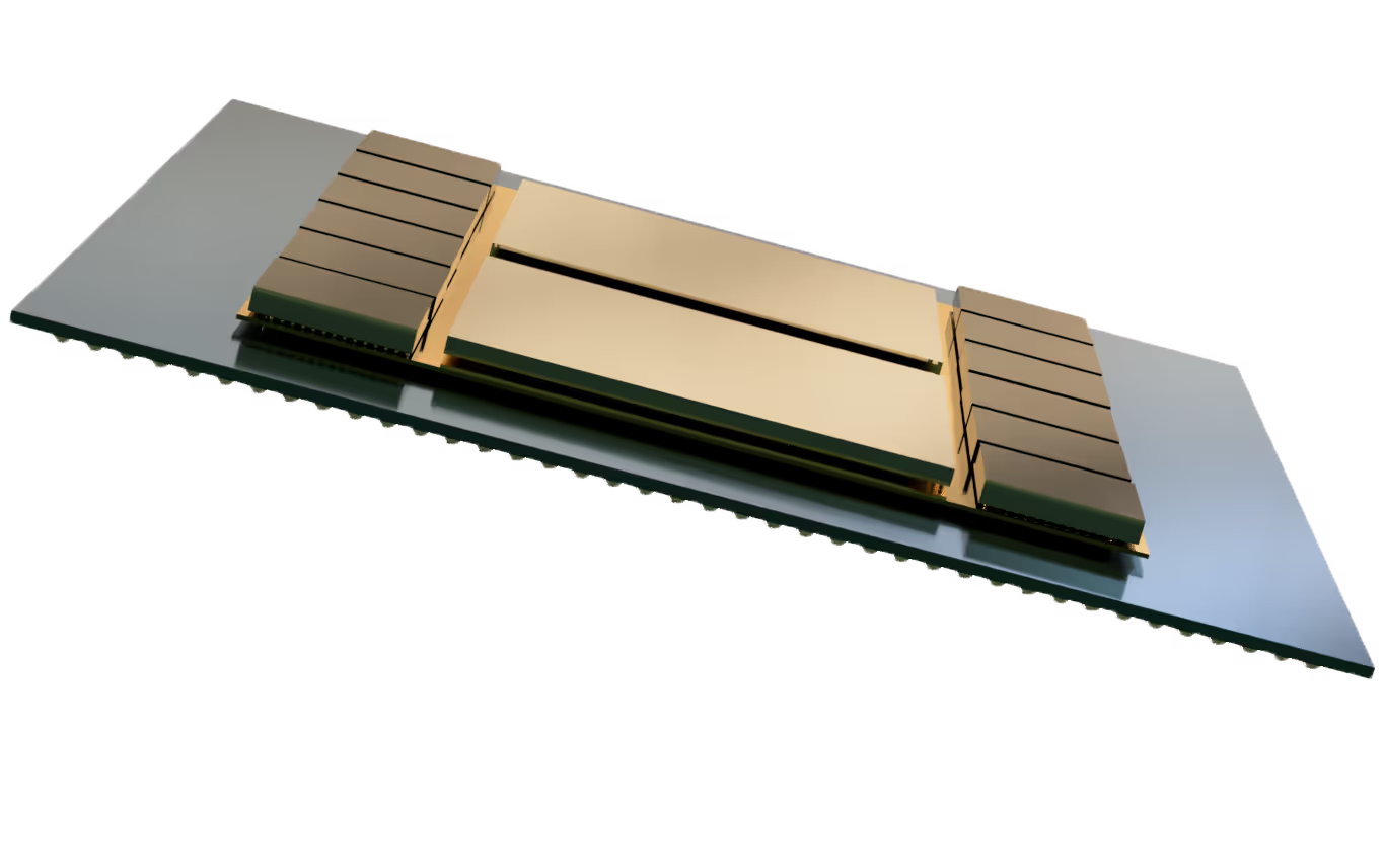
This chiplet architecture is inherently scalable and highly configurable, enabling seamless adaptation to any SoC power topology. Multiple chiplets can be deployed in parallel to construct the complete power delivery solution for a given SoC. Customers can implement power domains of varying shapes and sizes, optimized to the spatial and electrical requirements of the target system.
The chiplet’s z-height can be tightly controlled during fabrication, achieving targeted thickness in the low-hundreds-of-micrometer range. This flexibility supports multiple package integration schemes, from mounting at substrate land side to fully embedding in substrates or interposers.
Industry's first power delivery chiplet
PowerLattice’s pioneering power delivery chiplet integrates voltage regulation directly into the processor package. This chiplet is based on PowerLattice’s groundbreaking Rainier micro-IVR architecture that combines miniaturized on-die magnetic inductors, advanced control circuit innovations, a vertical design and a programmable software layer. It delivers the power at the closest place where compute happens with more than an order of magnitude reduction in power noise.
This results in more than 50% reduction of effective compute power needs, cooler and more reliable runtime, and less interference to high speed IOs. Under a fixed data center power budget, it can translate into 2X or more raw performance uplift.
Reinventing power delivery inside the processor
By delivering power inside the processor package, PowerLattice unlocks 2X or more performance per watt in scenarios where AI compute demand is limited by datacenter power and infrastructure constraints. This power solution also lowers cooling requirements and significantly extends processor lifetime.

PowerLattice’s solution is built for the world’s most demanding compute engines: AI accelerators, GPUs, and next-generation data-center processors


Our founders
- Dr. Peng ZouCEO & President
- Gang RenHead of Engineering
- Sujith DermalHead of Systems & Apps
Power design meets performance at scale


